Wireless GK Project
Version 3
Copyright (©) Harald Milz 2001
Put under the GNU General Public License (GPL)
See www.gnu.org.
This project starts to become more and more
concrete. If I haven't made any drastic thinking
errors the basic concept should be all right, and
there is nothing in it which makes it physically or
economically impossible. I am still looking for
serious fellow developers... :-)
Damn - the beast starts needing a name.
For all those poor AOL 4.0 users who can't save
HTML without crashing their machine: Here is a ZIP archive
of the whole folder.
Commercial disclaimer: I have no
commercial interest in this project, and do not
plan to market it. I would gladfully cooperate with
any capable firm to produce this unit, though, be
it a small startup or be it Roland if they ask me
kindly :-) Before you start to produce and market
these things be sure to read the GNU General Public
License, though. It requires you to put all derived
work under the GPL as well.
 A Different, Simpler
Approach
A Different, Simpler
Approach
Contents
The Roland GR synthesizer and its VG-8 companion
are incredible instruments. The dumbness of the
13-pin Atari monitor plug is incredible too. Either
you inadvertently rip out your cable from the GK
controller, or the cable wraps itself around a foot
pedal, or it starts to twist all along. It's high
time for a wireless GK cable. This is what this
proposal is about.
The 7 audio signals (guitar, GK string 1-6) are
ADC converted using low-power audio ADCs. The ADC
outputs are read by a microcontroller. Synth Vol is
voltage-to-duty-cycle converted read once per
frame, as well as S1/S2. The data is FM or MFM
modulated and sent via a wireless video link. The
receiver decodes the data and feeds the audio data
stream into 4 audio DACs. Synth Vol is restored, as
are S1 and S2.
The DIY project stops at the video signal output
and input, respectively. The DIY'er has to provide
his or her own video transmitter link
i.a.w. national regulations, as well as the power
source.
Expected performance:
- range about 300 m free air, 30 inside
buildings. That depends on the quality of the
video Tx/Rx set used. Buy the best you can afford!
- S/N > 90 dB, depends on the
ADC/DAC combo, and the error correction on the
RF link, as well as jitter and the quality of
the restored clock on the Rx side.
The video link will perform best in an
environment without much noise (what else is
new?). Everyone transmits on 2.4 GHz now. Diversity
receiver preferred, possibly in the 5.8 GHz ISM
band. Extremely expensive, it seems.
This is just a broad concept. Feel free to
comment, rip apart, rewrite, make up new ideas,
etc.
Block diagram see here. The transmitter
consists of
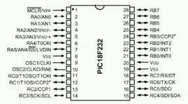
- a microcontroller PIC
18F232, 18F248/58,
or 18F242/52
@ 40 MHz. They are all pin compatible and
functionally identical as far as our needs are
concerned.
- 4 Stereo ADCs (Crystal Semiconductor CS53L32A
which consume typ. 28 mW @ 3V). After being
initialized by the PIC they run free, and in sync
because they use identical clock signals. The
ADCs run at 18 bits but we use only the 16 MSB in
some cases (need space to insert checksum and
other stuff). Should we use the ADCs' clip
detection? We could read the bit once per
frame. We have one spare ADC channel, and could
either use it for a microphone or to double the
guitar signal.
- a data encoder most of which is
implemented in software (PIC).
Synth Vol: we convert the 0..5V voltage to a 200-odd
Hz PWM signal with a duty cycle of 0..100%, and
read the single bit once per frame (sample rate ~
17 kHz). The generator consists of the usual
integrator/schmitt-trigger triangle/squarewave
generator and a comparator which compares the
triangle wave with the synth vol voltage. 3/4 of a LM324or
TL074, that is. The comparator output is read by
the PIC once every frame, i.e. the sample rate is
about 17361 Hz. That gives us an effective
resolution of ld(17361/200) or 6.4 bits.
S1/S2 are read by the PIC directly, and inserted
in the bit stream.
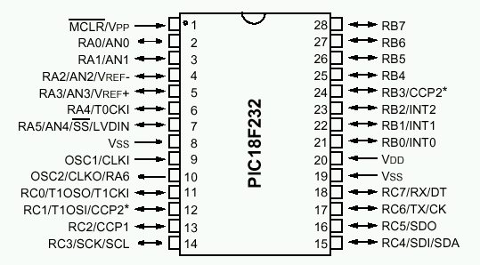
PIC 18F232:
- SPI output with external 5 MHz clock (the
PIC cannot create 5 MHz from the 40 MHz system
clock, no Fosc/8 capability).
- 40 MHz external clock
- Flash / ICSP (i.e. in circuit flashable)
- runs at 4V
- use weak pullup on inputs wrt. different Vcc
- AD converters switched off to save power
(ADON = 0)
- Port/Pin assignments:
        RA0 = /RST for ADCs
        RA1 = select for SPI -> ADCs
        RA2 = select for SPI -> transmitter module
        RA3 = LED
        RA4 = all /CS

        RB7 = Synth Vol PWM, ICSP DATA
        RB6 = ADC4 SDOUT, ICSP CLOCK
        RB5 = S2
        RB4 = ADC3 SDOUT
        RB3 = S1
        RB2 = ADC2 SDOUT
        RB1 = LRCK (uses INT1 to detect initial frame)
        RB0 = ADC1 SDOUT

        RC3/4/5 = SCK/SDO/SDI
        RC6/7 = USART Rx/Tx
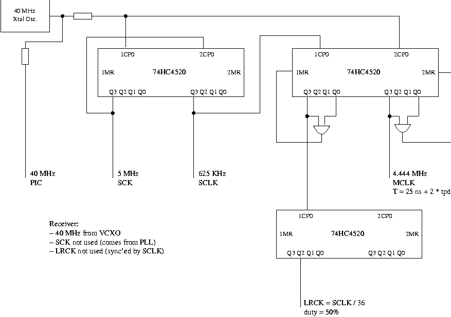
- all clocks are synchronous and depend on
each others so we can safely assume that timings
are fixed. Clock generation is basically the same
for Tx and Rx. External Xtal oscillator 40 MHz,
synchronous counters/dividers (see diagram):
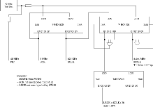 . I hope it'll work that way -
the 74HC4520
is specified as 68 MHz typ., 32 MHz min. ...
. I hope it'll work that way -
the 74HC4520
is specified as 68 MHz typ., 32 MHz min. ...
MF
SM370 needs about 7 mA @ 3.3V @ 40 MHz. The voltage
controlled counter part for the receiver would
be VC-SM570
(typ. 3.8 ps RMS jitter, up to 100 ppm pull range).
- 40 MHz / 8 = SCK = 5 MHz
- 40 MHz / 9 = MCLK = 4,444,444.4 Hz. The
CS4330 and CS53L32A data sheets do not
specify a duty cycle for MCLK!
- SCK / 8 = SCLK = 625 kHz
- SCLK / 36 = LRCK = 17361 Hz (sample rate)
REMARK: This sounds like a strange sample
rate but so what. The guitar signals are well
below 8 kHz. The 0.01dB passband edge is 0.4535*Fs = 7873
Hz. Use a passive lowpass to suppress
frequencies above SCLK/2 on input.
- ADC serial audio format 5 (right justified,
18 bit). Need to use control port mode for all
ADCs. That's still far better S/N and
linearity than using analog time or frequency
multiplex. It's 18 bits from a 24-bit ADC!
- then we have 16 clock cycles per loop left.
- release /RST on ADCs
- initialize SPI port (slave, idle=low, rising edge etc.)
- enable SPI to ADCs (RA1 = 1, RA2 = 0)
- /CS = 0
- initialize ADCs w/ SPI commands (write
only), clear PDN bit!
- switch SPI to external (RA1 = 0, RA2 = 1)
- set up INT vector for rising edge of LRCK
(RB1/INT1). we can also poll the beast
which is actually simpler.
- enable INT
- sleep (wait for next rising LRCK edge)
- ISR starts 3 - 4 instruction cycles after rising LRCK edge (latency)
- switch green LED on (RA3 = 1)
- disable INT1 (INT1IE = 0)
- Start cycle count. Once #36 is
reached, we're in sync.
- loop: 16 cycles == 1.6 µs (see below).
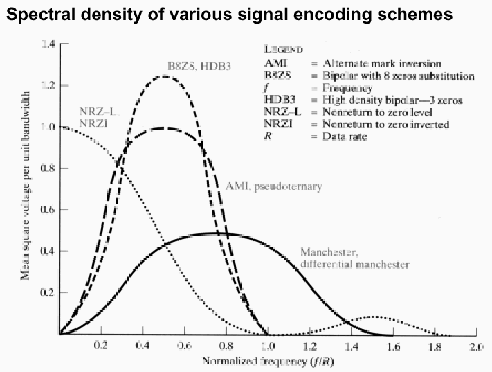
- The Miller Code (MFM) has the advantage of
using little bandwidth (see chart -- MFM is
similar to B8ZS, Biphase-Mark is similar to Manchester).
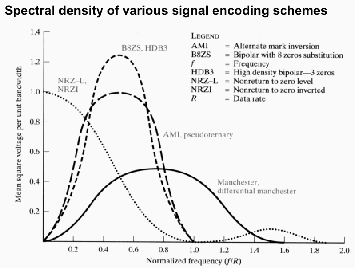
Miller encoding in software is fast and easy
if table lookups are used.
- 1 -> 01
- 0 after 0 -> 10
- 0 after 1 -> 00
Then you just need to add a positive edge
triggered D flip-flop to get the usual MFM
signal (HEF4013).
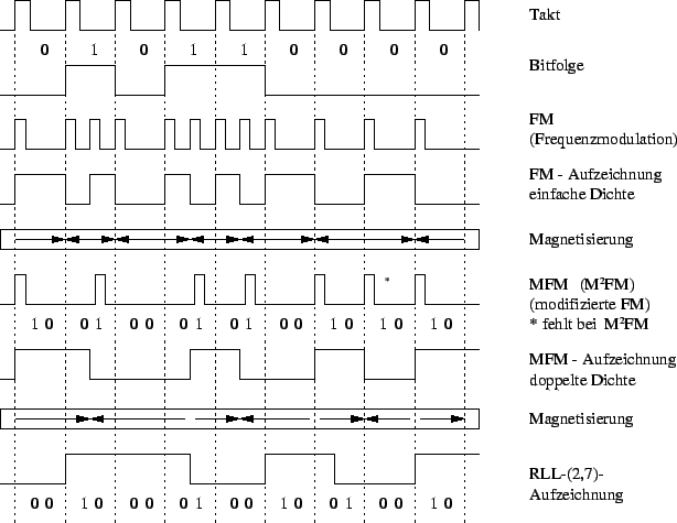
For a description of the encoding schemes
see also here.
Table lookup:
W:
a' b' c' d' a  b  c  d

X  X  X  0  0  0  0  0  -> 10 10 10 10
         0  0  0  0  1  -> 10 10 10 01
         0  0  0  1  0  -> 10 10 01 00
         0  0  0  1  1  -> 10 10 01 01
         0  0  1  0  0  -> 10 01 00 10
etc.
         1  1  1  0  1  -> 01 01 00 01
         1  1  1  1  0  -> 01 01 01 00
         1  1  1  1  1  -> 01 01 01 01
where a, b, c, and d are the 4 bits recently
read, and a', b', c' and d' are the 4 bits from
the previous read. We only need to keep d',
though, to determine what happens with a. The
perform a table lookup with the 5 LSB (i.e. 32
entries). Swap the nibbles and read the next 4
bits etc. That's it. It always takes the same
time no matter what the input is.
I'd try to implement M2FM to get
rid of the small DC offset MFM causes. This
should be achieved using a 64-entry table
lookup (we need to look at the 2 previous
bits).
- Simpler and cheaper alternative: use
biphase-mark code generated from simple FM
code. As you see in the bandwidth chart above, a
2.5 MHz biphase-mark signal fits nicely in the 5
MHz video bandwidth, and is DC free. It may even
be better than MFM because the FM bandwidth is
greater, and thus the S/N is better (is it? S/N
depends on the modulation index. FIXME). Due to
timing contraints in the PIC we'll never deal
with more than 2.5 MBit/s net data rate
anyway.
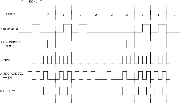
So we could simply read the 4 ADC
bits like
0a 0b 0c 0d
then OR
10 10 10 10 -> 1a 1b 1c 1d
then XOR to
the current checksum
then AND SCK and SDO (SCK
mode: CKP=0, CKE=1, i.e. idle low, rising edge),
and add a rising edge D FF (4013). The final
output signal lags by 100 ns. See chart:
For a discussion of spectral densities of
the modulations methods see also
To keep SDO busy all the time we need to write to
Port B after exactly 16 CPU clock cycles. According
to the PIC data sheet, writes to SSPBUF during an
active write are ignored. This could be solved by
using an external parallel-to-serial shift register
(74HC165)
and writing to Port B whenever we are done, or by
counting clock pulses very closely. /PL at
the falling edge of SCLK, shift with 5 MHz.
We'll add a 75 Ohm amplifier stage (e.g. LT1217)and a BNC
connector. The signal is attenuated to
2Vpp. If the video link breaks for some reason we
can use a cheap 75 Ohms RG-59B BNC-to-BNC cable.
Estimated power requirement:
| master clock | 25 mW |
| 4 * CS53L32A | 40 mW |
| PIC | 50 mW |
| several 74HC @ up to 40 MHz |
20 mW |
|
| Sum: | ~ 150 mW |
- use 4 AA size cells (NiMH, NiCD, alkalines,
rechargable alkalines, whatever)
- generate 4.2V for the PIC / 74HC and 3V for the
ADCs, respectively.
The ADCs could gain from a low-drop linear
regulator (MAX8862T). This
way, we can generate 3.15V / 100 mA for the
ADCs (OUT2) without external components, and
4.2V / 250 mA for the digital stuff (OUT1) with
a resistor divider. The efficiency is lower
than with a switched supply but the circuit
doesn't need inductors, and is simpler.
- generate appropriate voltage for video
transmitter
- if 5V type: use raw batt voltage
- if 12V type: use low-power step-up
converter MAX761. This
will be foreseen on the PCB but you don't
need to stuff the respective parts if you
don't need it. Max 150 mA are guaranteed but
the data sheet indicates we can pull about
300 as well. That should be enough for most
transmitters. If not, get a different one!
- generate ±7V for the GK controller from
the 4.2V line using DC-DC converter MAX864
(33 kHz). The chip is good for 20 mA which is
really enough.
- The MAX1779
seems to be a good choice for both the +5/12V and
±7V parts. Makes 13V/200 mA and up to ±40 V
20 mA. Low external parts count. :-)
It would be nice if all fit in a small case with a 4
AA cell battery compartment.
Most components should be SMD.
Everything should fit on a 80x100mm PCB (half Euro
card, that's what the freeware Eagle layouter can
provide), maybe a sandwiched 80x70mm daughter card
will be needed. Since the 13-pin PCB connector is
22 mm high including leads the case should be 24-25
mm high internally at least anyway. An alternative would
be to use no 13-pin PCB connector (who makes the
30cm 13-pin stub cable?) but permanently attach the
cable to the PCB. The PCB needs to provide a 14-pin
in-line plug too.
Using SMD components is a challenge for
soldering... The CS53L32A's pin pitch is 0.65mm
max. ...
If you prefer to stick the battery case in your
trouser pocket you can use a smaller case without
batt compartment (sounds like 110x90x30 mm). In
this case a lockable power connector is a must!
Block diagram see here.
The Input Stage will have 75 Ohm impedance. Input =
BNC connector.
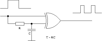
Use a fast comparator, like LM311, and a low pass
to create a floating reference. Positive feedback
to get a small hysteresis. Done.
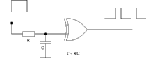 Biphase-Mark: use a XOR single-shot (74HC86,
T = 1.5/2*TSCK = 150 ns) to restore the FM signal
(2). This is handed to a edge-triggered VCXO PLL
(74HC4046 PC2) to keep clocks in sync. Use
restored SCK (3) to have PIC read SDI on rising
SCK edge (4). Register W contains 1a 1b 1c
1d. Odd numbered bits are ignored on
output, so just write to port. Done.
Biphase-Mark: use a XOR single-shot (74HC86,
T = 1.5/2*TSCK = 150 ns) to restore the FM signal
(2). This is handed to a edge-triggered VCXO PLL
(74HC4046 PC2) to keep clocks in sync. Use
restored SCK (3) to have PIC read SDI on rising
SCK edge (4). Register W contains 1a 1b 1c
1d. Odd numbered bits are ignored on
output, so just write to port. Done.
- Miller / MFM Decoder. The PLL restored clock is
used to control the master clock VCXO via another
4046 PLL. M2FM decoding can be
performed with the circuit described in US Patent
4612508. We're
still not commercial, are we? Preferably we'd
burn the circuit in a GAL to keep the part count
low, and make a more DIY reliable PCB.
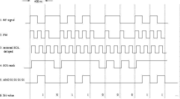
- MFM decoding in software: we could also
handle the input signal in a similar way like
biphase-mark, i.e. use a XOR gate w/ RC lowpass
to detect all edges, restore SCK via PLL, then
read into W, AND with 01 01 01 01, and
get 0a 0b 0c 0d - voilà. If no
bit errors occured, that is. The second half bit
is always identical to the encoded data bit. The
same is true for M2FM - so no
difference.
Same as above.
The algo needs to separate the digital audio data
and feed it to the DACs (2 LSB == 0). Frame sync
word -> LRCK. S1/S2 output to 2 port bits.
VCXO controlled by a PLL which pulls the clock
i.a.w. the received signal. This should produce a
very low jitter clock signal for the DACs.
The restored MFM or FM clock is 5 MHz so we need
to divide the VCXO frequency by 8. For
MCLK, SCLK and LRCK clock ratios see above.
- 4* CS4330. The
previously selected CS4227 and CS4327 don't
understand the CS53L32A's 18-bit, right-justified
signal (which in turn is the only 18-bit format
the CS53L32A understands). Alternatively (and if
easily available) we can use the pin-compatible
CS4339
which has slightly better THD and dynamic range
values, and offers anti-pop outputs. MCLK needs
to be 256x LRCK if we want to choose either DAC
interchangably.
- optional: Hush: SSM2000
for guitar signal. Does anyone think we need this
when the guitar signal is processed with 18 bits?
Or even if we use 2 ADC channels in parallel?
PCM, recovered by 1 Hz / 12dB/Oct low pass.
Output direct.
KISS: all linear. Everything is at +5V. -> 7805 /
LM340
(75 µV noise) or low noise replacement
(e.g. National
LP2989IMM-5.0 w/ 10 nF film cap as bypass, and
4.7 µF ceramic output cap -> 18 µV
output noise). Separate regulators for analog and
digital. Keep magnetic hum away: use separate wall
mart. This also helps avoid ground loops. The PCB
will only contain the rectifiers, capacitors and
regulators.
We'll take ±7V for some OPs from a
connected GK device.
3 GK outs w/ selector switch, and Guitar out
Not rackmount. We want to place the beast
near the GK footboxes (I wish Roland built
rackmount VG8 and GR-3X versions).
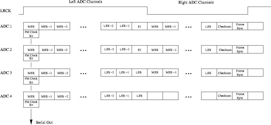
Since we need to read serial data streams from all
4 ADCs in parallel, and have hardly any time to
write the data to a indirectly addressed buffer
(18C242 manual pp. 50), we need to send the bits
via SSP immediately. Hence, the ADC-to-serial
protocol is very primitive. If anyone has a better
idea, ...
Frame sync: LRCK is read to determine the frame
sync. We produce a biphase-mark code violation, and
send 10 00 10 00 as the last byte of a
frame. There is no FM code which can produce this
pattern (FM has always the first half == 1). The
sequence is DC neutral too (even number of level
transitions, and equal distances between
transitions). The receiver will start a new frame
with the next received byte.
ADC4 has the guitar signal which is transferred
with full 18 bits (we could even use both ADC
channels for the guitar signal in parallel, and do
some checking in the receiver to reduce errors). GK
signals (ADC1-3) are handled with 16-17 bits "only".
S1/S2: are sent in bits 0 and 2 in cycle #18. We
do nothing special to the LSB and LSB-1 of ADC3,
and LSB-1 of ADC1 and ADC2 so effectively we
transmit the left phases with 17 and 18 bits,
respectively. Which strings should be have a better
resolution? The high ones or the low ones? We've
got 17, 17, 16, 16, 16, 16
Synth Vol: sent in bit 4 in cycle #18. Bit
errors are equalled by the low pass.
The transmitter routine has 3 special cycles:
#18, #35, and #36. These have to be checked in each
cycle. If we combine #35 and #36, and use registers
for the literals 18 and 35, we can save some
cycles.
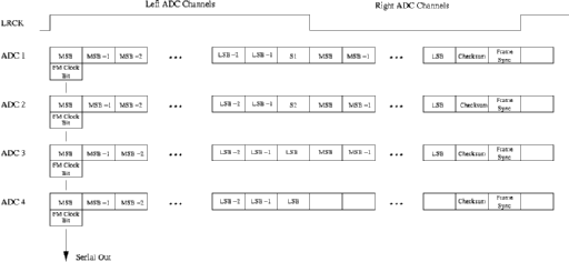
We thus have 144 bits per frame. Frame rate =
sample rate = 17361 Hz.
Checksum: the nibbles from cycles #1-34 are
XOR'ed against a RAM cell which was nulled on the
last frame sync. This RAM cell thus accumulates an
XOR parity. In cycle #35, the parity is sent. This
simple scheme will detect all odd number bit errors
in each of the 4 parallel bit streams. It will not
correct anything so we just discard false messages,
and repeat the previous one.
Since we can't correct any errors as of yet,
this is rather error recognition than error
correction. I'd like to be able to correct at least
single bit errors. We could use Hamming
code which makes 7 bits from 4 bits but then
we'd have to generate the MFM encoding
externally. Hamming code is simple to generate
(table lookup) but not so easy to decode with a few
CPU cycles.
Links:
Any more tips & tricks appreciated. Maybe
someone can write a Reed-Solomon Decoder that
uses only 3 PIC instruction cycles or so :-)
The 18C PICs have 3 indirect adressing pointers
so we can
Raw program logic:
read consecutive data bytes and wait for frame
sync. In the meanwhile, restore start values for
the variables above.
- poll SSPSTAT,BF (2 TCY)
- if not cycle #34 (actually it's #35 because we
use PREINC counters, and haven't incremented
yet; CPFSEQ = 1 TCY if != 34)
- the first thing we do is
retrieve a nibble from PREINC1 (now the cycle
counter is correct), write to port
(this nibble is from the latest correct
frame). (MOVFF, 2 TCY, so after 500 ns we
effectively write the received data, and must
make sure the external SCLK isn't any faster
:-)
- read SSPBUF (1 TCY)
- store in PREINC0 (1 TCY)
- XORWF the result to the current checksum (1
TCY). We ignore the odd numbered clock bits
- they will XOR to the same values in the
transmitter and receiver.
- if ! cycle #18 : loop. (CPFSEQ, GOTO loop =
3 TCY)
- else (cycle #18) (1 TCY), write bits 0
and 2 to S1 and S2, and bit 4 to synth vol (AND, write = 2
TCY). Since these bits are null most of the
time we simply write them to ADC1 and ADC2 as
well. This is not true for the synth volume
bit #4! S1 and S2 need to be on a port
different from RB because RB is written in
each cycle. LRCK = 0. (1 TCY, must happen as
late as possible) GOTO loop (2 TCY)
- else (is #34 - 3 TCY if = 34)
we combine #35 and #36 to have 32 TCY for
everything.
- write 0x00 to RB (2 TCY). The data will
remain there until #1 of the next frame
- read SSPBUF (1 TCY) and store in PREINC1
(now FSR1L = 35) (1 TCY). XOR against stored parity
from PREINC0 (1 TCY)
- if it's correct (CPFSEQ, BRA INCORRECT, 1 TCY), swap
FSR0H and FSR1H (4 TCY), reset warning LED "parity
error" (1 TCY) and continue (2 TCY) with
swapped buffers.
- else incorrect (Z flag != 0, 3 TCY)
leave FSR0H and FSR1H intact, set warning LED
"parity error" (1 TCY) and continue, hence
discard previous contents of buffer 0, and
write buffer 1 to the ADCs once more.
- continue: poll SSPSTAT,BF (2 TCY) We
need a timeout here!!!
- read SSPBUF (1 TCY) should now contain
frame sync. We're now in #36.
- if frame sync (2 TCY if =) reset warning
LED "RF sync loss" (1 TCY) and continue (BRA,
2 TCY)
- else (we are in cycle #36 and didn't
receive frame sync. What if we received frame
sync and we aren't in cycle #36?) set warning
LED "RF sync loss", and wait for the next
frame sync. continue. Not timing critical any
more, until we find a new frame sync.
- continue: FSR0L = FSR1L = 0, XOR checksum
buffer = 0, LRCK = 1 (as late as possible).
(4 TCY) loop (2 TCY)
Many conditionals... 16 clock cycles must be
sufficient for that. The Scenix SX CPUs
have only one (!) INDF and FSR register each, and
hence we cannot use 2 buffers as shown above. Argh.
How do people get preprogrammed PICs and GALs? Not
everyone will be able to program the 2 PICs and the
GAL.
Someone suggested to do diversity on the
demodulated end of the receiver(s) (a.k.a. "True
Diversity"). This is independant of the other stuff
and can be built in addition to the single
receiver. More design ideas are here. This
would require
- 2 or 3 low-cost receivers of the type above,
all running on the same RF channel.
- 2 or 3 video OPs with enable (e.g. OPA3355). Their
common output is routed to the demodulation
circuit described above. Soft switching would
make sense to avoid clicks. Maybe even a 74HC4066
is sufficient (max on-channel bandwidth 160 MHz,
crosstalk -80 dB @ 1 MHz, off-channel isolation
-40 dB @ 1 MHz).
- 2 or 3 full wave rectifiers to measure the
video signal strength at the demod outputs. Since
the rectified signal has a bandwidth of about 1
MHz the low pass time constant can be in the low
millisecond range.
- A 5..10 MHz bandpass per receiver to detect
noise whenever the FM signal strength is too low
- a microcontroller (e.g. PIC with AD
converters) to choose the strongest receiver
after a certain dead time and with a floating
hysteresis. A 20 MHz PIC (e.g. 16F85/86)
is fast enough to provide a detection cycle time
in the millisecond range. Algorithm suggestions
welcome!
- If we limit ourselves to using 2 receivers
(what most commercial systems do) the detector /
switch part can be replaced by hardware (2 field
strength detectors, Schmitt Trigger with floating
hysteresis and delay, 2-channel video OP w/
enable (e.g. OPA2680).
Or does someone have a working application for the
Analog Devices AD6600?
http://www.dynapix.com/supertriad.htm ?
A very interesting system is S-515P on http://www.cocom.com/acatalog/Online_Catalog_CVT_500_29.html. A
bit expensive for hobbyists maybe.
In order for the user to be able to upgrade the devices'
firmware without special tools (ICSP capable
programmer), we need to use the USART port and
write some code to do the programming.
Sample code is contained in Microchip's Application
Note TB025 "Downloading HEX Files to PIC16F87X
PICmicro ® Microcontrollers". The code is specific
for the PIC 16F87X types but can be ported to using
the TABLE instructions of the 18F quite easily.
Basically, we add a MAX233
(no external caps needed) to convert the USART port
to a "real" RS-232 port because we cannot assume
all serial ports work with unipolar +5V voltage
levels. The MAX233 uses about 5mA without load, so
we sort of switch its Vcc off if we don't need
it. The same switch can inform the PIC that serial
programming is now enabled.
Software: we enable the USART interrupt in the
init routine, and set the corresponding IRQ vector
to the serial programming routine. When data
arrives, it will be accepted by the programming
routine, and written to program memory using the
TBLWT instruction. The code needs to make sure it
isn't overwritten itself. It'll use software
handshaking. To save power, we
deactivate the USART as long as it isn't actually used (SPEN
= 0).
Firmware upgrades will be available on the web
in Intel HEX file (INHX8M) format. This is what MPASM and GPASM
create and support. Everyone can download the code
and simply send it to the device using a standard
PC and serial port no matter what operating system
is used. Data rate will be 19200 bps 8N1 - higher rates
are not standardized, and 38400 is not available @
40 MHz clock.
Thus, the devices need to have a 9-pin serial
connector. Will be used with a normal serial
cable, not a null modem cable.
This is only for the non-developers. People who
build the devices themselves are supposed to have a
ICSP capable PIC programmer.
I normally use the Eagle layout
editor and autorouter for which there is a free
demo version. It can only produce 80x100 mm PCBs
though, as part of the shareware limit. The full
license costs only $49, though. Layout files will
be distributed as Eagle files (.sch and .brd).
For those Linux users among you (like me), see
Microchip's
statement about Linux support. Basically, go to
www.gnupic.org. I
for one will be using GPASM on
Linux. GPASM is rather comprehensive. It does not
officially support the 18F232 yet but the
18C242. These two aren't much different as far as
can be seen from the very brief 18F232 data sheet.
For other platforms than Linux you may need to
get a copy of MPASM, or use GPASM
with a Cygwin environment if you're a Windoze
l00Z3R ;-)
During the development stage, the GNU PIC
Simulator GPSIM
may be extremely helpful. Supposedly, it doesn't
fully support the 18Cxxx family yet but as far as I
can see from the GPSIM source code all that we need
should be there. GPSIM should save a lot of
EEPROM/Flash burning cycles, and we can test the
correct timing before touching the solder iron at
all.
To program the initial stuff into the PIC
(serial programming routine), one needs a ICSP
capable programmer. The PCBs will contain a 5-pin
ICSP header. See the Microchip
ICSP Programming Guide
Debugging can be done by adding some code which
writes to the serial port, and connecting a PC to
the MAX233. If the PC has 2 serial COM ports we can
supervise both Tx and Rx at the same time.
I'm listing only German sources here.
- PICs: Farnell (not 18F by now) or
http://www.rutronik.com/produkte/index.html
(incl. 18Fx58)
- Crystal:
Atlantik Elektronik
- PIC, 74HC: http://www.arrow.com/ via Sasco or
Spoerle
You can use any commercially available video
transmitter/receiver combo you like and you can
afford, in whatever frequency range is appropriate
(800 MHz, 2.4 GHz, 5.8 GHz, you name it). Use one
with the highest RF output power you can get.
Over time, we will try to compile a list of
appropriate video transmitters.
Hint: if
your transmitter / receiver has a separate audio or
even switch channel you can add a Reset button
which resets both the transmitter's and the
receiver's PIC! Just in case...
- Conrad pp. 519/882.
- the Gigalink module offers 5 selectable channels.
-> use alarm switch connector for S1/S2 ?
-> use microphone input for synth vol VCO signal
-> hence only 7 audio channels over video FM.

ELV (www.elv.de): 4-Kanal-Sendesystem ALM 2442 399 DM (set!)
- transmitter uses 4.8..7.2V, i.e. Vbat directly.
- has audio channel (reset)
- can use a case w/ 4 AA-cell battery compartment.
- batt cptmt: Conrad 521868 or external battery
  pack w/ cable
- also nice: Bopla BOS 752 or 807
  (http://www.bopla.de/, w/ 4 AA-cell
  battery compartment) (Reichelt pg 179/80)


https://spynet.xynx.com:
- auch 25 mW Minisender.  (auch Gigalink - 2004311, 390 DM)
- angeblich nur 120 mA
- Mini TX II 10 oder 25 mW (?) 2200012  480 DM
- Empfänger 2048020 229 DM (COnrad 329 DM)

-> non-diversity :-(

http://www.securitec-gerlach.de/: very
  cheap. Quality?

http://www.dynapix.com/oem.htm ? Only signel
  frequency, needs 500 mA!

Diversity:
http://www.premierewirelessinc.com  5.8 GHz

I have got one hint saying the cheap X1 transceivers
work fine for SPDIF (http://www.x10.com/products/offer105.htm)
- Having little experience with SMD - does it
make sense to place decoupling capacitors and
similar components on the back side of the PCB
(current flows through the vias) or is it better
to place them side by side with the components
that need decoupling?
I was asked why I dropped my old proposal which
involved analog frequency modulation, companders
etc. Well - too many knobs to tune, not really DIY
safe.
To my other
electronic projects
Harald Milz
Last modified: Thu May 31 20:54:15 CEST 2001
 . I hope it'll work that way -
the 74HC4520
is specified as 68 MHz typ., 32 MHz min. ...
. I hope it'll work that way -
the 74HC4520
is specified as 68 MHz typ., 32 MHz min. ...
 Biphase-Mark: use a XOR single-shot (74HC86,
T = 1.5/2*TSCK = 150 ns) to restore the FM signal
(2). This is handed to a edge-triggered VCXO PLL
(74HC4046 PC2) to keep clocks in sync. Use
restored SCK (3) to have PIC read SDI on rising
SCK edge (4). Register W contains 1a 1b 1c
1d. Odd numbered bits are ignored on
output, so just write to port. Done.
Biphase-Mark: use a XOR single-shot (74HC86,
T = 1.5/2*TSCK = 150 ns) to restore the FM signal
(2). This is handed to a edge-triggered VCXO PLL
(74HC4046 PC2) to keep clocks in sync. Use
restored SCK (3) to have PIC read SDI on rising
SCK edge (4). Register W contains 1a 1b 1c
1d. Odd numbered bits are ignored on
output, so just write to port. Done.